PCIe PCB Layout Guidelines: Essential Tips for Designers Designing pcie interfaces and extenders « adafruit industries – makers ...
If you are looking for PCB Routing Guidelines - Part 12 (PCIe signals) you've visit to the right web. We have 25 Images about PCB Routing Guidelines - Part 12 (PCIe signals) like PCIe Gen 6: PCB Design Essentials | EMA Design Automation, Designing PCIe interfaces and extenders « Adafruit Industries – Makers and also PCIE-PCB设计规范!(建议收藏)-CSDN博客. Read more:
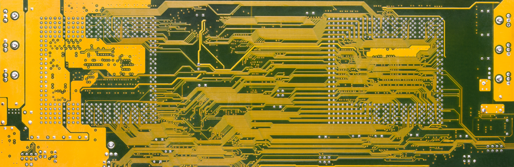
PCB Routing Guidelines - Part 12 (PCIe Signals)
 embeddeddesignblog.blogspot.com
PCB Routing Guidelines - Part 12 (PCIe signals)
PCB Layout Guidelines And Considerations
 www.microcontrollertips.com
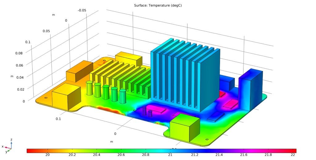
PCB layout guidelines and considerations
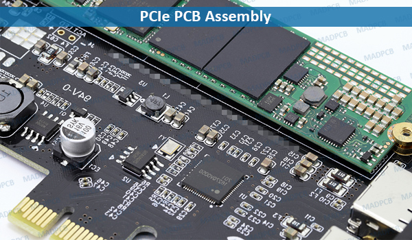
PCI Express: PCIe PCB Manufacturing, Assembly, Design | MADPCB
 madpcb.com
PCI Express: PCIe PCB Manufacturing, Assembly, Design | MADPCB
PCB Design Tutorial: Basic Rules, Tips And Guidelines-TechSparks
 www.tech-sparks.com
PCB Design Tutorial: Basic Rules, Tips and Guidelines-TechSparks
PCIE-PCB设计规范!(建议收藏)-CSDN博客
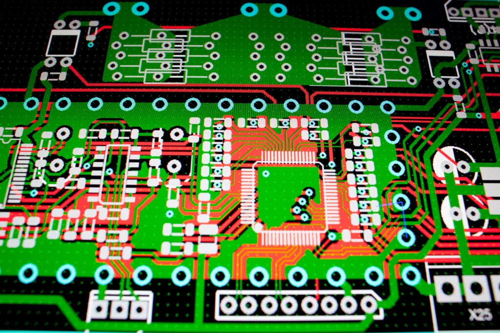
PCIE-PCB设计规范!(建议收藏)-CSDN博客
PCI And PCIe In PCB Layout Design-ELEPCB - ELEPCB
 www.elepcb.com
PCI and PCIe in PCB Layout Design-ELEPCB - ELEPCB
Essential PCB Silkscreen Guidelines For Layout
 www.linkedin.com
Essential PCB Silkscreen Guidelines for Layout
PCB Layout Editor: Essential Features And Best Practices – Hillman
 hillmancurtis.com
PCB Layout Editor: Essential Features and Best Practices – Hillman ...
PC & PCI Cards - Multi Circuit Boards
 www.multi-circuit-boards.eu
PC & PCI cards - Multi Circuit Boards
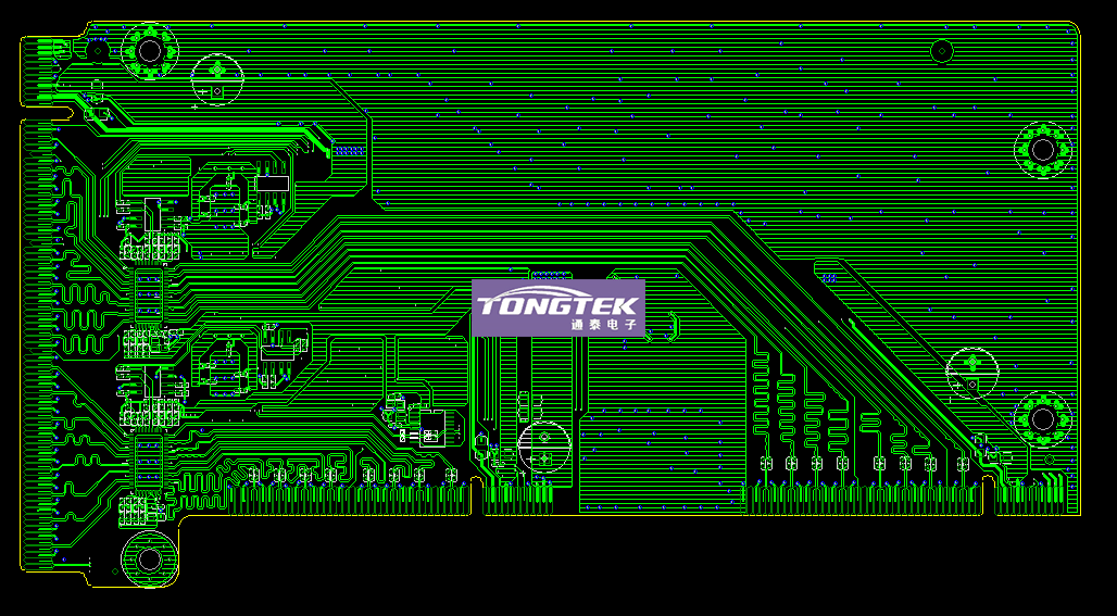
PCIE转接板 - PCB设计案例 - 通泰电子
 www.tontektech.com
PCIE转接板 - PCB设计案例 - 通泰电子
PCIe Gen 6: PCB Design Essentials | EMA Design Automation
 www.ema-eda.com
PCIe Gen 6: PCB Design Essentials | EMA Design Automation
Impedance Matching - PCB Design For High-frequency Differential Lanes
 electronics.stackexchange.com
impedance matching - PCB design for high-frequency differential lanes ...
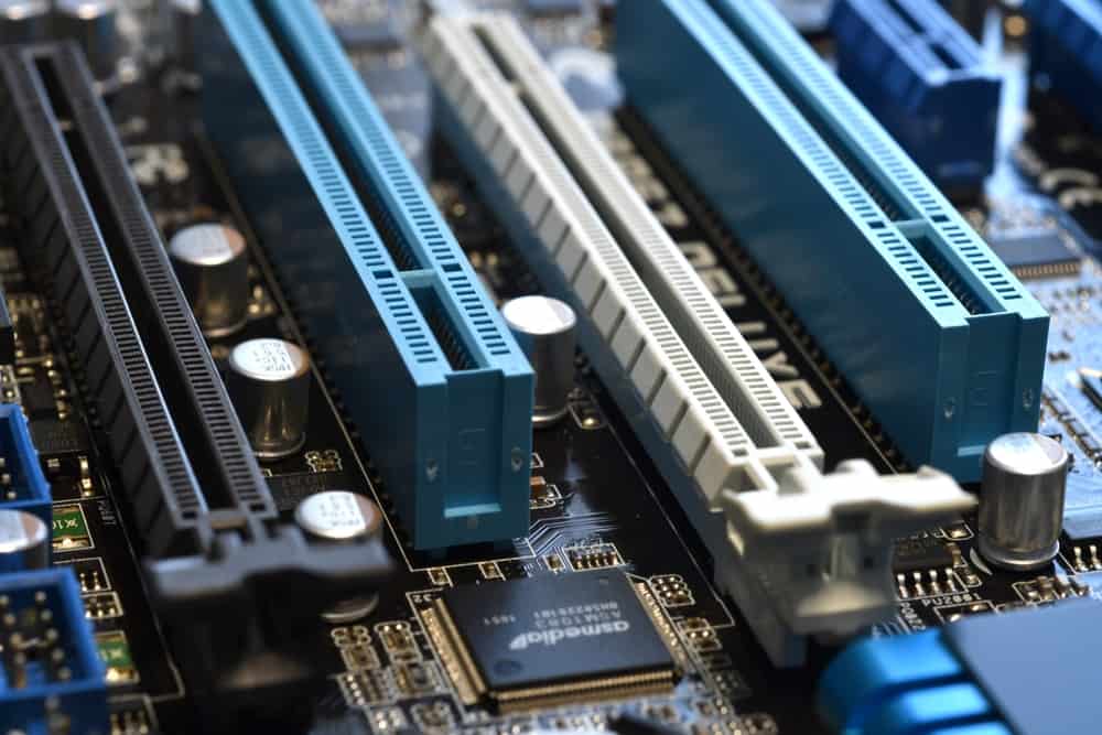
Designing PCIe Interfaces And Extenders « Adafruit Industries – Makers
 blog.adafruit.com
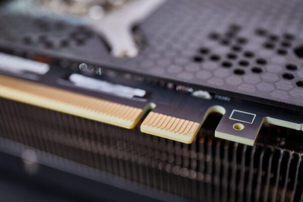
Designing PCIe interfaces and extenders « Adafruit Industries – Makers ...
PCIe Gen 6: PCB Design Essentials | EMA Design Automation
 www.ema-eda.com
PCIe Gen 6: PCB Design Essentials | EMA Design Automation
PCIe In PCB Design: Layout And Routing Guidelines | Blog | Altium Designer
PCIe in PCB Design: Layout and Routing Guidelines | Blog | Altium Designer
PCIe Gen 6: PCB Design Essentials | EMA Design Automation
 www.ema-eda.com
PCIe Gen 6: PCB Design Essentials | EMA Design Automation
PCIe Gen 6: PCB Design Essentials | EMA Design Automation
 www.ema-eda.com
PCIe Gen 6: PCB Design Essentials | EMA Design Automation
PCIe Gen 6: PCB Design Essentials | EMA Design Automation
 www.ema-eda.com
PCIe Gen 6: PCB Design Essentials | EMA Design Automation
Review Of Server PCB Layout & Schematic - Part 4: PCI Express (PCIE
 www.youtube.com
Review of Server PCB Layout & Schematic - Part 4: PCI Express (PCIE ...
PCB Layout Rules For PCIE, SATA, LAN, LVDS, USB, SDVO,
 www.fedevel.com
PCB layout rules for PCIE, SATA, LAN, LVDS, USB, SDVO,
PCIe Routing Guidelines: Overview | EMA Design Automation
 www.ema-eda.com
PCIe Routing Guidelines: Overview | EMA Design Automation
PCIe In PCB Design: Layout And Routing Guidelines | Blog | Altium Designer
 resources.altium.com
PCIe in PCB Design: Layout and Routing Guidelines | Blog | Altium Designer
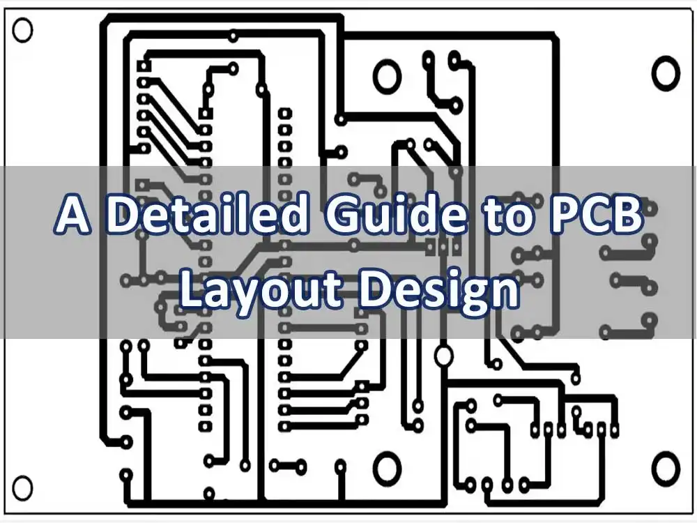
Complete Guide To PCB Layout Design Steps And Rules Circuit Diagram
 declanstarling.pages.dev
Complete Guide To PCB Layout Design Steps And Rules Circuit Diagram ...
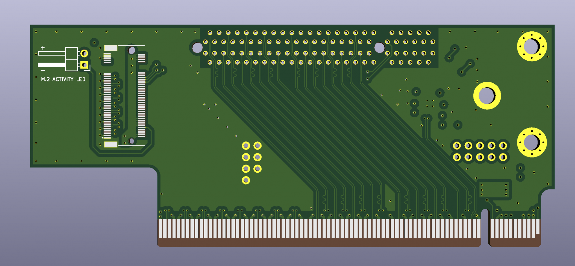
Rolling Your Own PCIe Bifurcation Riser – Matt's Tech Pages
 www.mattmillman.com
Rolling your own PCIe Bifurcation riser – Matt's Tech Pages
PCIe Routing Guidelines & Best Practices - Free Online PCB CAD Library
 www.ultralibrarian.com
PCIe Routing Guidelines & Best Practices - Free Online PCB CAD Library
Impedance matching. Pcie in pcb design: layout and routing guidelines. pcie routing guidelines: overview